Nano Materials Research Lab
Thin Film Processing Facilities (NMRL)
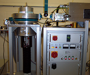
iPLAS MPCVD System |
|
 |
|
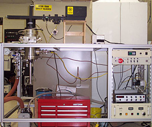
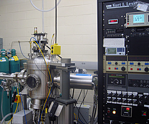
ASTeX MPCVD System |
|
 |
|
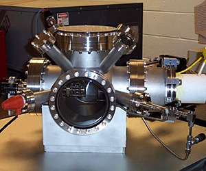
Pulsed Laser Deposition System |
|
 |
|
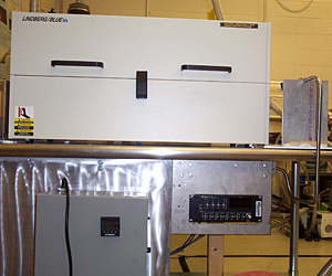
Carbon Nanotube Growth Facility |
|
 |
|
CMS-18 Sputtering System with Load Lock |
|
 |
|
Metrology and Characterization Facilities(NMRL)
Renishaw MicroRaman Spectroscopy |
|
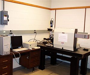 |
|
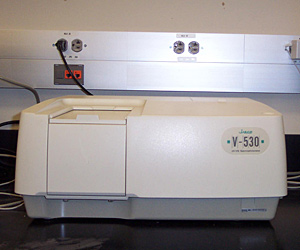
FTIR Spectroscopy |
|
 |
|
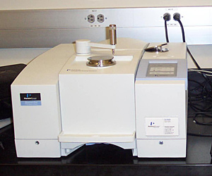
UV-VIS Spectrophotometer |
|
 |
|
Micro Manipulator 6000 series probe station |
|
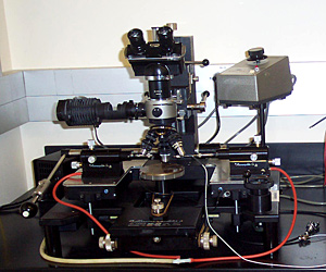 |
|
Agilent 4294A Impedance Analyzer |
|
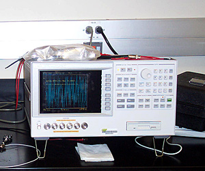 |
|